Neighbors thought he was just a retired shopkeeper. But a police visit revealed cash everywhere — and a “loophole” that’s technically legal. 📍 Madrid, Spain — June 2025 A 62-year-old
Neighbors thought he was just a retired shopkeeper. But a police visit revealed cash everywhere — and a “loophole” that’s technically legal. 📍 Madrid, Spain — June 2025 A 62-year-old

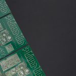
Imagine a world where your electronic devices can adapt instantly to new tasks, troubleshoot themselves, or even optimize performance on the fly—all without needing a complete redesign. That’s the power of programmable logic today, and at the heart of this revolution are Field-Programmable Gate Arrays, or FPGAs. These versatile chips are transforming the way engineers and innovators approach adaptive electronics, making devices smarter, more flexible, and incredibly customizable. So, what exactly is an FPGA? Think of it as a gigantic Lego set for electronics. Unlike traditional chips that have a fixed function, FPGAs are like blank canvases filled with programmable blocks called logic elements. You can connect these blocks in countless ways, effectively creating your own custom digital circuit tailored to any application. Once configured, they perform the specific tasks you need with high speed and efficiency. And if your project calls for changes later, no problem—just reprogram the FPGA, and it adapts accordingly. This flexibility makes FPGAs ideal for platforms demanding rapid prototyping and evolving requirements. For instance, in aerospace and defense, where systems must be highly reliable yet adaptable to new threats or mission profiles, FPGAs provide the agility researchers need. They can update or modify functionalities in the field, reducing costly downtime and hardware redeployment. Likewise, in telecommunications, FPGAs help manage increasing data traffic, handle protocol upgrades, and optimize signal processing dynamically. What makes FPGAs even more compelling is their ability to integrate diverse functions—analog, digital, and even embedded processors—on a single chip. This capacity enables the development of sophisticated adaptive systems that can process sensor data, run machine learning algorithms, and communicate seamlessly with other components—all in real time. For example, in advanced robotics or autonomous vehicles, FPGAs can be the brain that quickly interprets sensor inputs and makes split-second decisions, ensuring safety and performance. The evolution of FPGA technology continues apace, with newer models offering higher densities, lower power consumption, and enhanced programmability. Development tools have also improved, making it more accessible for software engineers and hardware designers to work together in creating these adaptive systems. Open-source projects and intellectual property cores further democratize FPGA design, fostering innovation across industries. In a nutshell, FPGAs are the cornerstone of modern adaptive electronics, turning static hardware into dynamic, intelligent systems. Whether it’s shrinking the size of data centers, empowering next-generation communications, or enabling smarter consumer gadgets, programmable logic unlocks endless possibilities. As technology marches forward, expect FPGAs to become even more integral, making our devices more flexible and capable than ever before. So, if you’re into building the future of electronics, understanding FPGAs might just be your first step into a truly adaptable world.
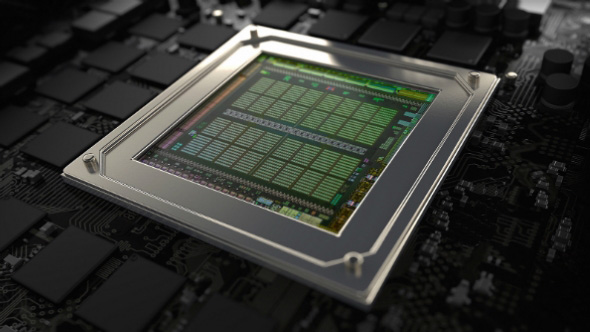
**Chips for Autonomous Systems: How Embedded AI Optimizes Edge Decisions** Let's face it—autonomous systems have become the brains behind many of our modern gadgets and vehicles. From self-driving cars to drones, these systems rely heavily on embedded artificial intelligence (AI) chips that are specifically designed to handle complex decision-making right at the edge, where the data is actually generated. But what makes these chips different from traditional processors? And how do they make autonomous systems smarter and more efficient? Let’s dive into the world of embedded AI chips and find out! First off, embedded AI chips are specialized hardware components optimized to run AI algorithms locally—without having to send data back and forth to the cloud. This local processing is crucial when milliseconds matter, like avoiding a sudden obstacle on the road or navigating unpredictable terrain. Relying solely on cloud computing can introduce delays, internet connectivity issues, or security concerns. Embedded AI chips tackle these challenges head-on by providing rapid, on-device decision-making power. One of the key features of these chips is their architecture. Unlike general-purpose CPUs, embedded AI chips often employ neural network accelerators or digital signal processors (DSPs), tailored to efficiently perform the matrix and vector operations common in AI workloads. By dedicating hardware to these tasks, they can execute complex algorithms much faster and with lower power consumption—extending the battery life of drones or autonomous vehicles. Let’s take self-driving cars as an example. Their embedded AI chips process data from various sensors—cameras, LIDAR, radar—in real-time to identify objects, predict behaviors, and make navigation decisions. This requires processing vast amounts of data quickly, sometimes within fractions of a second. High-performance chips like NVIDIA’s DRIVE Orin or Tesla’s custom AI chips are designed specifically for these purposes, ensuring the vehicle can react instantly to changing situations. In addition to speed, energy efficiency is a big deal. Autonomous systems often run on limited power sources, especially drones or mobile robots. Embedded AI chips utilize advanced fabrication technologies, such as processes with a 7nm or 5nm node, to pack more computational power into less space while consuming less energy. This balance of power and efficiency allows these devices to operate longer and perform more complex tasks without overheating or draining their batteries. Another exciting trend is the integration of these chips with other system components. Many embedded AI solutions now come as System on Chips (SoCs), combining multiple functionalities—processing cores, memory, communication interfaces—on a single piece of silicon. This integration reduces latency, simplifies design, and cuts costs, making autonomous systems more affordable and reliable. But it’s not just about raw processing power. The software stack running on these chips is equally important. Lightweight, optimized AI frameworks like TensorFlow Lite or proprietary accelerators ensure that models run smoothly on edge devices. Companies are also developing tools to help developers optimize models specifically for these chips, squeezing out every bit of performance. All of this means smarter, faster, and more reliable autonomous systems. Whether it’s a drone scouting for forest fires, a robot sorting packages in a warehouse, or a driverless car navigating busy streets, embedded AI chips are the unsung heroes running the decision-making engine right at the edge. In a nutshell, chips for autonomous systems are revolutionizing how machines perceive, interpret, and interact with the world. By bringing AI computations close to the data source, they not only improve response times and safety but also open the door to a future where smarter machines operate seamlessly around us. And as technology continues to advance, expect these chips to become even more powerful, efficient, and integral to our everyday lives.

Over the past year, optical sensors in smartphones have seen a pretty exciting evolution, transforming the way we interact with our devices daily. If you’re into tech or just love having the latest gadgets, you’ve probably noticed how much smarter and more capable these tiny components have become. Let’s take a quick tour through the technical changes that have been shaping the optical sensor landscape over the last year. First up, we saw major improvements in under-display optical fingerprint sensors. These aren’t just about making the fingerprint scanner invisible; they’re now faster, more accurate, and capable of working through thicker screens. Some of the latest sensors employ optical sub-systems that combine multiple LEDs and photodiodes to enhance image quality and speed. This means unlocking your phone is now almost instantaneous, even in challenging lighting conditions. Furthermore, manufacturers are exploring multi-sensor arrays to increase security and reduce false matches, a step forward from earlier implementations that sometimes struggled with dirt or moisture. Another significant shift has been the refinement of ambient light sensors. While they’ve been around for years, their role has become more sophisticated, particularly with the advent of adaptive displays. Modern sensors can now dynamically adjust the screen brightness, color temperature, and even refresh rates based on ambient lighting and user activity. This doesn’t just improve battery life but also enhances user comfort. Some high-end models incorporate multi-element sensors that better detect flickering and ensure consistent color rendering, even under changing lighting conditions. Camera optical sensors have also undergone notable advancements. These sensors are now more sensitive, with higher pixel counts and improved quantum efficiency, leading to better low-light performance. The integration of computational photography techniques relies heavily on these sensors’ capabilities. Over the past year, manufacturers have been pushing the envelope by embedding multi-layer stacked sensors, which enable faster readouts, improved HDR imaging, and real-time video processing. Some flagship devices now feature sensors with global shutters—that means less motion blur and better handling of fast-moving objects—making mobile photography more like professional DSLRs. Likewise, time-of-flight (ToF) sensors, which help with depth mapping, AR experiences, and portrait effects, have become more precise and power-efficient. Recent iterations include multi-layer structures and improved IR illumination, making 3D sensing quicker and more accurate even in low-light scenarios. This helps achieve more realistic background blurring in portrait mode and more accurate depth data for AR applications. Finally, sensor fusion technology has gained traction. This combines data from multiple optical sensors to produce richer, more accurate information—think better face recognition, improved image stabilization, and smarter autofocus. With AI algorithms increasingly integrated into the hardware, the synergy between optical sensors and software continues to push what’s possible on smartphones. All in all, the last year has been a whirlwind of innovation in optical sensors. They’ve become faster, more precise, and more capable, all while maintaining energy efficiency and durability. This technological evolution not only contributes to sleek and responsive devices but is also setting the stage for a new wave of features—think seamless AR, supercharged photography, and biometric security that’s almost foolproof. If this pace keeps up, who knows what we’ll be showcasing in smartphones a year from now?
Sure! Here's an excerpt for your article on "Mobile GPUs: Balancing Energy Efficiency and Performance" in an informal, informative style: --- When it comes to mobile devices—be it your smartphone, tablet, or a sleek gaming laptop—the graphics processing unit (GPU) plays a crucial role in delivering smooth visuals and immersive experiences. But unlike desktops with unlimited power supplies and ample cooling, mobile GPUs have a tricky job: they need to deliver impressive performance *without* draining your battery or overheating your device. So, how do manufacturers strike that delicate balance between energy efficiency and performance? Well, it all comes down to smart engineering and innovative technology. First off, mobile GPUs are designed with power consumption in mind. They’re built to be more energy-conscious than their desktop counterparts by using lower voltage levels, simplified architectures, and clever power management techniques. For instance, many mobile GPUs include multiple "performance states"—think of these as gears in a car—and can dynamically switch between them depending on what you're doing. When you're just browsing social media or streaming videos, the GPU might operate at a low power state, conserving energy. But when you're gaming or rendering demanding visuals, it ramps up to reach higher performance levels. Manufacturers also leverage cutting-edge fabrication processes, like smaller transistor nodes (such as 7nm or 5nm tech), to reduce power consumption without sacrificing speed. These smaller processes allow more transistors to fit on a chip, making it faster and more efficient simultaneously. Another important aspect is software optimization. Developers optimize gaming and graphics applications to make the most of mobile GPUs’ capabilities, ensuring they use resources efficiently. Features like variable refresh rates (think of these as adjusting the frame rate on the fly) help smooth out visual transitions and prevent unnecessary power draw. However, there's always a bit of a trade-off. Cranking up performance often leads to increased energy use and heat generation, which isn't ideal in the confined spaces of mobile devices. That’s why next-gen mobile GPUs focus on adaptive performance—scaling their power up or down based on demand—to maintain a good balance. Think of it like driving a car: you can’t always go full throttle, but with the right control, you can merge speed with fuel economy. In the high-performance category, gaming and AI workloads push mobile GPUs to their limits. Manufacturers like AMD, NVIDIA, and ARM are developing specialized architectures—like NVIDIA’s GeForce RTX for mobile and ARM’s Mali series—that aim for maximum punch without sacrificing too much battery life. The result? Devices that can handle demanding games or intensive tasks, while still lasting through your day. All in all, the evolution of mobile GPUs is all about smart compromises. Developers continue to refine hardware and software to give us the best possible experience without the constant worry about battery drain or overheating. The future? Expect more energy-efficient designs, smarter power management, and even more capable mobile graphics that let you game, stream, and create on the go—all without sacrificing your device’s longevity. --- Let me know if you'd like me to make any adjustments or add more details!

Sure! Here's an excerpt for your article on "Quantum Algorithms in Cloud Systems: A 2025 Technical Outlook": --- **Quantum Algorithms in Cloud Systems: A 2025 Technical Outlook** By 2025, the landscape of cloud computing is set to experience a seismic shift, thanks to the rapid maturation of quantum algorithms integrated within cloud platforms. If you’ve been keeping an eye on quantum tech, you know it’s no longer just a playground for academia—major cloud providers are actively rolling out quantum-enabled services that promise to revolutionize data processing, optimization, and cryptography. So, what’s the big deal with quantum algorithms in this space? For starters, quantum algorithms harness phenomena like superposition and entanglement to tackle specific problems exponentially faster than classical algorithms. Think of complex optimization problems, drug discovery, and material simulations—all of which are crucial for industries like finance, healthcare, and manufacturing—being upgraded to run on cloud-based quantum processors. By 2025, cloud platforms such as AWS, Azure, and Google Cloud are projected to offer accessible, scalable quantum computing resources. This democratizes access to powerful quantum algorithms, empowering developers and researchers to experiment without needing their own costly quantum hardware. These platforms are expected to feature hybrid quantum-classical workflows—approaches where classical systems handle routine tasks, while quantum modules take on the heavy computational lifting for specific problems. One notable trend is the refinement and deployment of algorithms like Variational Quantum Eigensolvers (VQE) and Quantum Approximate Optimization Algorithm (QAOA). These algorithms are designed for near-term quantum computers—called Noisy Intermediate-Scale Quantum (NISQ) devices—and are optimized for cloud integration. They’re already showing promise in solving combinatorial optimization problems, a common bottleneck in logistics and supply chain management. Another big breakthrough expected by 2025 is the development of quantum error correction techniques embedded within cloud services. While quantum computing is still fragile—errors in qubits can cascade—cloud providers are investing heavily in creating more stable, reliable quantum environments. These advances will result in higher fidelity computations, making quantum algorithms not just experimentally interesting, but practically usable across real-world applications. Security is also shifting in the quantum realm. Cloud-based quantum services feature quantum key distribution (QKD), promising theoretically unbreakable encryption. As quantum algorithms evolve, so will the methods to safeguard sensitive data, making security protocols more robust in our increasingly interconnected world. Overall, the year 2025 marks a pivotal point where quantum algorithms are transitioning from theoretical constructs to practical tools within cloud ecosystems. Whether it’s optimizing complex logistics, simulating new materials, or enhancing secure communications, the fusion of quantum computing and cloud infrastructure is set to unlock capabilities we’re only beginning to imagine. Keep an eye on these developments—they’re shaping the future of computing, faster and more accessible than ever before. --- Let me know if you'd like me to tailor it further!
Sure! Here's an excerpt for your article on "Next-Generation Solid-State Storage: Where Engineers Are Heading," written in an informal, informative style within the specified character range: --- If you've been around tech circles lately, you've probably heard a lot of buzz about the future of solid-state storage. It’s no secret that SSDs have revolutionized how we store and access data — from blazing-fast laptops to giant data centers. But the real fun is just beginning. Engineers are now pushing the boundaries beyond traditional NAND flash, exploring new materials, architectures, and technologies to create storage solutions that are faster, more durable, and more energy-efficient. One of the biggest players on the horizon is **3D XPoint** (or Intel Optane), which sits somewhere between DRAM and NAND in terms of speed and durability. Think of it as a sweet spot — blazingly fast, with a much longer lifespan than typical NAND chips. This tech allows for ultra-low latency, meaning data can be accessed almost instantly, reducing bottlenecks in data-heavy scenarios like AI training or high-frequency trading. But it’s not just about incremental improvements. Engineers are working hard on **storage class memory (SCM)** that blurs the line between memory and storage. The idea is to have a single tier that can both serve as super-fast cache and persistent storage, simplifying architecture and boosting performance. Companies are experimenting with materials like phase-change memory, resistive RAM (ReRAM), and ferroelectric RAM (FeRAM), all of which promise faster speeds, lower power consumption, and better endurance. Another hot area is **solid-state drives built with new architectures**, like 3D stacking and chiplets, which essentially build storage chips layer by layer to pack in more capacity. Think of it as stacking LEGO bricks to make a bigger, smarter storage tower. This not only boosts capacity but also reduces latency because data doesn’t have to travel far inside the chip. Then, there’s the push towards **energy-efficient storage solutions**. Data centers consume an enormous amount of power, and sustainable tech is a big focus. Engineers are working on materials and designs that can operate at lower voltages and generate less heat, helping to cut down on cooling costs and environmental impact. Lastly, emerging technologies like **quantum storage** are also being explored — though they’re still early-stage. Imagine storage devices that leverage quantum effects for nearly instant data retrieval, which could revolutionize everything from cloud computing to cryptography. All these innovations might sound futuristic, but many are already hitting the prototype stage or are in the early days of commercial deployment. The goal is clear: create solid-state storage that’s faster than anything we’ve seen, more reliable, and better aligned with the ever-growing demands of data-driven industries. As engineers continue to tinker and refine, the next-gen storage landscape promises a future where data speeds and capacities are limited only by our imagination. --- Would you like me to expand on any specific technology or aspect?

Hey there! Let’s dive into a fascinating topic that’s rapidly changing the way we connect and interact with our gadgets—neural network computing and its huge impact on the future of the Internet of Things (IoT). You might have heard of neural networks as being behind AI advancements like voice assistants and image recognition, but their role in IoT is shaping up to be even more exciting. So, what exactly is neural network computing? Think of it as teaching computers to mimic how our brains work—learning from data, recognizing patterns, and making decisions just like humans do. Unlike traditional computer programming, which is all about rules and instructions, neural networks adapt and improve over time. They process tons of data from sensors, devices, and users, and use that to get smarter. Now, bring this into the world of IoT—which is basically a huge network of connected devices like smart thermostats, wearable gadgets, autonomous cars, industrial sensors, and more. These devices generate massive amounts of data every second. The challenge? Making sense of all that info quickly and accurately, often in real time. That’s where neural network computing comes in. It enables these devices to analyze data locally or via cloud processing with much better accuracy, leading to smarter decision-making. One game-changer is how neural networks help with predictive analytics. For example, in smart homes, sensors monitor energy use, and neural networks can predict when appliances will need maintenance or suggest optimal energy-saving settings. In health tech, wearable devices can analyze data patterns to warn users about potential health issues before they become serious. Industrial IoT systems use neural networks to predict machinery failures, minimizing downtime. The result? Not only do devices become smarter; they also deliver more personalized, proactive experiences. Moreover, advances in neural network hardware—like specialized chips optimized for AI computations—are making it possible to deploy these complex models directly on edge devices. This means IoT gadgets can process data locally, reducing latency, saving bandwidth, and increasing privacy because sensitive info doesn’t always need to travel to the cloud. This edge computing approach is crucial for applications that require instant responses—like autonomous cars avoiding obstacles or health monitors alerting emergency services immediately. Looking ahead, the symbiosis between neural networks and IoT is set to explode. With the increasing sophistication of neural network models—like transformer architectures that are already transforming natural language processing—we’ll see even more intuitive, context-aware IoT gadgets. Imagine smart cities where traffic flow is optimized in real-time, energy grids that adapt dynamically, and public safety systems that detect hazards instantly—all powered by advanced neural network computing. However, challenges remain, such as managing energy consumption for large models, ensuring data security, and avoiding biases in AI algorithms. Researchers and developers are actively tackling these issues, pushing towards more efficient, ethical, and reliable solutions. In essence, neural network computing is revolutionizing IoT from a simple connected device ecosystem into an intelligent, adaptive universe that learns and evolves. As these technologies mature, expect our everyday interactions with the digital world to become more seamless and personalized—making smarter cities, healthier lives, and more efficient industries a real possibility. Pretty exciting, right?

Imagine a world where you no longer have to fuss with tangled cords or constantly plug and unplug your devices. That’s the promise of wireless power—an exciting tech frontier that’s edging closer to everyday reality. But how exactly does it work, and what are the practical steps we can take to make wireless power a part of our daily lives? Let’s dive into the basics and some actionable steps to get there. First, understand that wireless power primarily relies on two main technologies: inductive charging and resonant inductive coupling. Inductive charging is the most common—you’ve probably seen it in action with some smartphones and electric toothbrushes. It works by creating a magnetic field between a charging pad and your device. When they’re close enough, energy transfers from one to the other, charging your battery without any cables involved. Resonant inductive coupling takes it a step further; it allows power transfer over slightly larger distances and with more flexibility, which is crucial for practical everyday use. So, what can we do to push wireless power into our routines? For starters, device manufacturers need to keep adopting and standardizing these technologies. The {Qi} standard, for example, has become a universal norm for wireless charging, making devices compatible across brands straightforward. When shopping, look for gadgets that support Qi or similar standards—it's the first practical step towards embracing wireless power. Next, infrastructure matters. Think about furniture, office environments, even public spaces—integrating wireless charging pads into tables, desks, and streets can make charging as simple as placing your phone down. Some startups and tech giants are already experimenting with “power mats” installed in cafés or airports. The key is for businesses and homeowners to retrofit their spaces with these energy zones, turning everyday spots into ‘charging hotspots’ without cluttering them with cables. Another crucial step is policymaking and collaboration between tech companies and regulators. Currently, wireless power technology is advancing fast, but standards and safety protocols need to keep pace. Governments and industry groups can facilitate this by funding research, setting safety standards, and promoting interoperability. That way, users can trust that their devices are being charged safely and effectively in diverse settings. And let’s not forget about the potential for smart energy management. Wireless power systems could be integrated into home automation, allowing devices to charge when needed and even optimizing energy use. Think of your living room with a hidden energy “grid” that automatically powers your gadgets as they need it—more convenience, less waste. Of course, challenges remain, like efficiency losses over distance, compatibility issues, and costs. But these are hurdles worth tackling. Advances in materials like graphene and better coil designs are already improving transfer efficiency. As technology matures, prices will drop, making wireless power more accessible. In the end, the practical realization of wireless power in our daily lives demands a mix of technological innovation, thoughtful infrastructure development, supportive policies, and consumer awareness. By taking these steps, we’re moving toward a future where charging is effortless and cables become a thing of the past. So, whether it’s a wireless charging pad at your desk or power-enabled furniture at your favorite café, the future of wireless power is closer than you think—and it’s ready to transform how we keep our devices alive and kicking, every day.
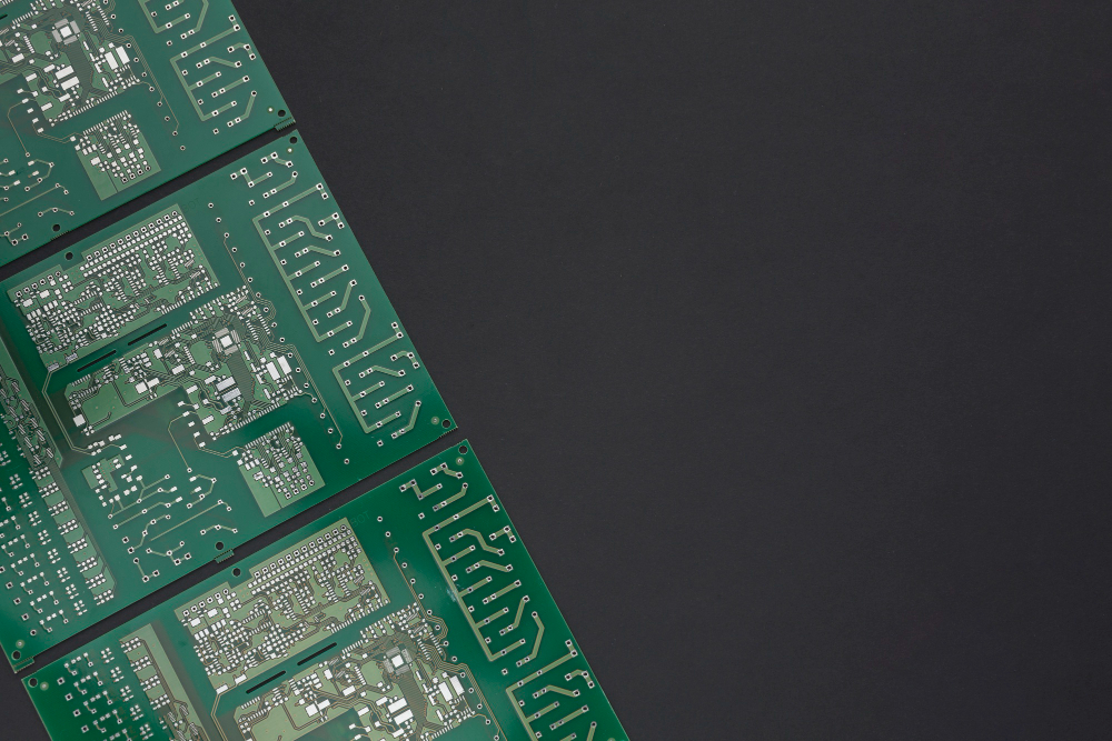
Sure! Here's an engaging excerpt for your article on how new microprocessors are reshaping modern device architecture: --- In the rapidly evolving world of tech, microprocessors are like the unsung heroes powering everything from your smartphone to complex data centers. Over the years, advances in microprocessor design have fundamentally changed how devices are built and operate, making them faster, smarter, and more efficient than ever before. So, what’s new on the microprocessor front, and how is it shaking up device architecture? First off, let’s talk about the shift toward **multi-core processors**. Instead of relying on a single, lightning-fast core, manufacturers now pack multiple cores into a single chip. This helps devices handle multitasking better—think streaming, gaming, and running background apps all at once—without breaking a sweat. It’s a game-changer for everything from smartphones to laptops. But it’s not just about cramming more cores in; it’s about smarter cores too. Recently, we’ve seen the emergence of **heterogeneous architectures**, where different types of cores are combined within the same processor. For example, ARM’s big.LITTLE design pairs high-performance cores with power-efficient ones. This way, devices can switch between cores depending on the task—saving battery during light use but ramping up performance when needed. Another biggie is **specialized processing units** integrated alongside traditional CPUs. Think of AI accelerators or neural processing units (NPUs). These tiny but mighty chips are tailored to handle machine learning tasks, making AI features more responsive and less of a drain on resources. This shift essentially frees up the main processor to focus on general tasks, boosting overall device efficiency. The push for **energy efficiency** continues to drive innovations. Modern microprocessors are more power-conscious, employing techniques like dynamic voltage and frequency scaling—aka DVFS—to tailor power use in real time. The result? Lighter, longer-lasting devices without sacrificing performance. Then there’s the advent of **chiplet architecture**. Instead of designing monolithic chips, engineers now assemble processors from smaller, modular chips called chiplets. This approach not only allows for greater scalability and customization but also reduces manufacturing costs and improves yields. Finally, the integration of **advanced manufacturing processes**, such as 3nm and beyond, means that microprocessors are getting smaller and more densely packed than ever. These tiny leaps in process technology boost performance and efficiency, paving the way for more powerful, compact devices. All these innovations together are turning the traditional device architecture on its head. With microprocessors now smarter, more adaptable, and more efficient, the devices we rely on daily are becoming faster, more capable, and more energy-friendly. As we look ahead, these trends hint at a future where our tech gadgets will be not just smarter but seamlessly integrated into every aspect of our lives. --- Let me know if you'd like me to adjust the tone or focus!